
The convergence of mobile systems-on-chip and desktop central processing units has reached a major inflection point with recent synthetic performance metrics. Data extracted from an early Apple A20 Pro benchmark indicates a profound shift in single-threaded execution capabilities across personal computing. While mobile processors historically relied on tightly constrained thermal envelopes to preserve battery longevity, advanced semiconductor manufacturing nodes now allow aggressive architectural scaling that directly challenges legacy x86 architectures. This fundamental evolution represents far more than a routine increase in operational clock frequencies. Instead, it marks a deliberate structural re-engineering of general-purpose mobile computing topologies across the global semiconductor industry.
Understanding the trajectory of modern silicon requires examining the physical manufacturing foundations provided by advanced semiconductor foundry partners. The ongoing industry transition toward cutting-edge extreme ultraviolet lithography has reshaped what design teams can realistically achieve within pocketable hardware form factors. When analyzing raw performance scaling across successive hardware generations, physical limits of transistor density, interconnect resistance, and energy efficiency dictate the boundaries of mobile computation. As chip designers push higher operational frequencies into passively cooled mobile environments, balancing dynamic power consumption and thermal dissipation becomes the defining engineering challenge of the decade.
Previous silicon generations were primarily characterized by steady but incremental performance gains that closely tracked standard process shrinks. For instance, the step from four-nanometer manufacturing to early three-nanometer nodes yielded modest baseline improvements across flagship mobile processors. The architectural leap observed in current two-nanometer designs, however, departs significantly from that conservative performance trend. By leveraging nanosheet gate-all-around transistor geometry, leading foundry processes dramatically diminish parasitic capacitance and off-state current leakage, enabling high-performance central processing unit cores to sustain elevated clock speeds under heavy burst operating conditions.
These physical manufacturing improvements translate directly into tangible computational capabilities across both single-threaded and multi-threaded workloads. The ability to drive higher instruction throughput without triggering immediate power spikes fundamentally alters how operating systems allocate tasks between specialized processing blocks. As a result, modern application processors can handle complex background tasks, real-world instruction pipelines, and heavy computational demands with unprecedented responsiveness, setting up a new paradigm for how mobile hardware compares to traditional desktop workstations.
In early synthetic testing within the Geekbench 7 suite, the processor achieved 4,006 points in single-thread evaluations and 11,460 points in multi-thread tests. These specific metrics represent a 23.3 percent improvement in single-thread execution and a 27.1 percent increase in multi-thread capability when compared directly against the preceding A19 Pro generation. The magnitude of this generational jump underscores how a foundational process node shrink combined with aggressive microarchitectural optimization can reset performance expectations across the broader consumer electronics ecosystem.
Decoding the Apple A20 Pro benchmark architecture
A deeper analysis into the underlying silicon layout reveals that the six-core system architecture utilizes two dedicated general-purpose super cores running at clock speeds reaching up to 4.93 GHz, complemented by four high-efficiency cores designed to manage continuous background tasks. This central compute cluster is supported by a thoroughly redesigned memory subsystem that allegedly features a 96-bit memory I/O interface, delivering a 50 percent increase in total memory bandwidth compared to prior designs. Higher memory throughput is crucial for feeding wider execution pipelines and preventing core starvation during instruction decoding.
The structural design of these high-performance super cores relies on front-end pipeline expansion, expanded instruction caches, and refined branch prediction algorithms that mirror execution engines found in workstation silicon. In single-thread benchmark evaluations, the chip demonstrates a 7.1 percent performance lead over the workstation-grade M5 processor, matching an identical 7.1 percent increase in peak clock frequency. This direct alignment suggests that mobile application processors are now deploying high-performance CPU core designs identical to those utilized in laptop and desktop systems, effectively erasing historical architectural separation.
When compared against high-power desktop central processing units, the single-thread benchmark figures present a striking technical contrast. The mobile processor leads AMD’s 16-core Ryzen 9 9950X3D by 26 percent and Intel’s Core i9-14900KS by 32 percent in single-threaded operations. While x86 desktop processors maintain clear advantages in multi-threaded workloads due to higher core counts and sustained power budgets exceeding 170 to 253 watts, the ability of a smartphone system-on-chip to outperform desktop hardware in single-threaded tasks highlights the efficiency of modern ARM microarchitectures.
To fully grasp these structural changes, analysts must examine how instructions pass through execution units during burst calculations. Desktop chips traditionally achieve top single-thread performance by drawing significant dynamic voltage and operating near thermal limits. In contrast, modern mobile super cores utilize wide decode windows and massive out-of-order execution buffers to maximize instructions per cycle at lower operational voltages. This design shift allows the chip to achieve record-setting single-core scores during brief test cycles before thermal accumulation forces clock speed throttling.
Within the flagship smartphone landscape, the performance gap between rival mobile platforms has widened significantly across synthetic measurements. The chip outperforms competing flagship platforms, including Qualcomm’s Snapdragon 8 Elite Gen5 and Xiaomi’s XRing O3, by margins ranging between 31.5 percent and 33.7 percent in single-thread benchmarks. Technical analysis of those rival processors indicates their single-thread scores remain comparable to two-year-old mobile silicon designs like the A18 Pro, illustrating how aggressive core scaling can create multi-year performance leads.
Competitive ecosystem disparities and laptop convergence
In multi-threaded evaluations, the six-core mobile processor continues to demonstrate surprising competitiveness against higher core count competitors. It leads the eight-core Snapdragon 8 Elite Gen5 by 12.2 percent and achieves multi-threaded performance roughly equivalent to the ten-core Xiaomi XRing O3. Furthermore, when compared against MediaTek’s eight-core Dimensity 9400, the chip posts a 76 percent advantage in single-thread and a 48 percent advantage in multi-thread tests. Against Google’s Tensor G5, the leads expand to 99 percent in single-thread and 96 percent in multi-thread capabilities.
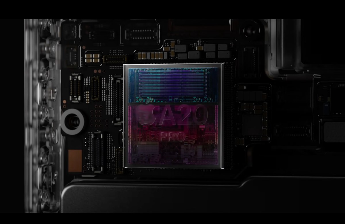
The performance variance is even more pronounced when examining chips developed under strict fabrication constraints and geopolitical restrictions. Compared to Huawei’s Kirin 9050 Pro, the chip demonstrates a 290 percent lead in single-thread execution and a 139 percent advantage in multi-thread throughput. This vast disparity highlights how access to leading-edge foundry nodes, as detailed in recent A20 Pro performance analysis reports, creates an escalating competitive barrier for semiconductor designers operating on older manufacturing processes.
The single-thread performance trajectory of this mobile system-on-chip extends directly into comparisons with dedicated laptop processors as well. In single-core testing, the chip is 7 percent faster than the M5, 20 percent faster than the M4, and 43 percent faster than the M3 processor. Because of its six-core topology, its multi-threaded capabilities naturally lag behind ten-core laptop designs, trailing the M5 by 39 percent and the M4 by 27 percent. However, it remains within 5 percent of the multi-thread score of the eight-core M3 processor, proving mobile chips can match prior laptop compute capabilities as discussed in iPhone silicon architecture evaluations.
Comparisons with x86 mobile offerings reflect a similar structural pattern across mainstream PC platforms. Against Intel’s Panther Lake architecture, the chip achieves a 48.7 percent higher single-thread score than the flagship Core Ultra X9 388H, even though the 16-core Intel chip delivers 63 percent higher multi-threaded throughput. When measured against mainstream mobile processors like the Core Ultra 5 325 and Core Ultra 5 332, the mobile chip delivers 74 to 88 percent faster single-thread performance while maintaining a 3 to 64 percent advantage in multi-threaded workloads, demonstrating a seismic realignment in personal computing silicon.
Thermal dynamics and real-world execution constraints
Despite these extraordinary synthetic benchmark figures, serious technical constraints must be evaluated regarding real-world sustained application performance. Synthetic benchmarks like Geekbench primarily measure burst computation, executing short mathematical operations that allow high-performance CPU cores to ramp up to peak clock speeds without saturating the physical thermal capacity of the host device. In a smartphone form factor, passive heat dissipation relies entirely on internal vapor chambers and chassis surface radiation, which places strict limits on heat dissipation over extended timeframes.
Operating two super cores at 4.93 GHz generates concentrated heat density that rapidly pushes thermal junction limits toward critical thresholds. In sustained workload scenarios, such as continuous three-dimensional graphics rendering, complex video encoding, or extended mobile gaming, smartphone power management systems must aggressively reduce operational clock frequencies to prevent hardware degradation and maintain safe chassis touch temperatures. While a desktop processor can draw hundreds of watts supported by active liquid cooling, a mobile system-on-chip operates within a sustained power budget capped between 5 and 8 watts.
Consequently, while single-thread synthetic scores prove microarchitectural superiority in short execution bursts, sustained performance will inevitably experience thermal throttling over extended durations. This divergence between peak burst capability and sustained thermal capacity represents the primary engineering dilemma for modern smartphone hardware. Mobile platforms can briefly outperform high-wattage desktop processors in brief tasks, but maintaining those operational states requires external cooling or larger physical chassis enclosures, as documented across public Google News publication index coverage detailing mobile hardware trends.
Understanding the boundary between burst metrics and sustained workloads is essential for software engineers building demanding cross-platform applications. Software designed for mobile devices must be structured around asynchronous execution and aggressive power state switching to leverage burst single-core speed without causing thermal throttling. Algorithms that assume continuous high-frequency execution will quickly trigger power throttling, resulting in performance degradation after initial execution bursts. Hardware capabilities have advanced, but software design choices dictate real-world outcomes.
The decision to integrate desktop-grade super cores into a smartphone application processor aligns with a strategic unified architecture philosophy. By maintaining structural core consistency across mobile operating systems and desktop platforms, software developers can optimize instruction pipelines and memory allocation for a single core microarchitecture. This unified approach simplifies cross-platform software compilation, accelerates localized machine learning inference workloads, and enhances overall software ecosystem cohesion across varied hardware tiers.
As semiconductor manufacturers push further into sub-three-nanometer nodes, the capital expenditure required for silicon design and physical mask set production continues to climb exponentially. Reusing unified super core designs across smartphone application processors, tablet chips, and desktop systems allows companies to amortize massive research and development expenses across vast production volumes. This economic reality ensures that high-volume mobile silicon will continue driving foundational architectural innovations for the entire semiconductor industry.
Looking ahead, the long-term impact of integrating desktop-class core topologies into passive mobile environments will depend on breakthroughs in advanced packaging technology and internal power delivery. Multi-die chiplet arrangements, integrated voltage regulators, and backside power delivery networks will become necessary to maintain energy efficiency as core counts and clock speeds increase. The gap between theoretical burst benchmark performance and real-world sustained workload execution will remain the central boundary defining mobile processor design for years to come.