
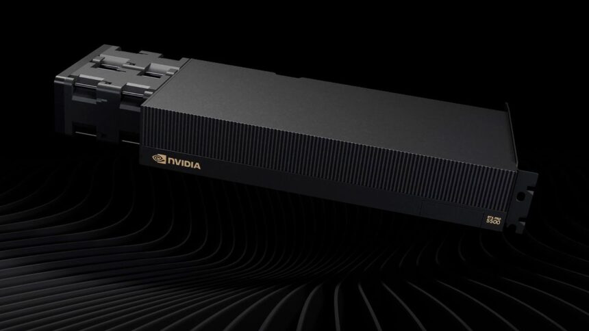
The enterprise artificial intelligence landscape faces a persistent structural tension between computational throughput and physical memory capacity. Large language models and multi-modal neural networks require extensive frame buffers to store parameters locally without incurring severe latency penalties from offloading to host memory. To address this operational constraint, the Nvidia RTX Pro 5500 pairs 84GB of high-speed GDDR7 video memory with enterprise Blackwell silicon. By deploying high-density memory configurations on harvested flagship processing dies, chip designers can capture substantially higher commercial margins while providing specialized accelerators for machine learning researchers. This release illustrates how hardware manufacturers strategically redirect high-end silicon into enterprise channels to meet institutional demand.
Commercial allocation strategies consistently prioritize professional computing nodes over consumer gaming hardware during periods of intense artificial intelligence expansion. While flagship consumer graphics cards share their physical die foundations with enterprise workstation boards, memory deployment strategies establish distinct functional tiers. Understanding how silicon harvesting, circuit layout, and memory bus parameters interact exposes the real engineering choices governing modern workstation hardware. Technology procurement teams tracking hardware updates often follow broader industry shifts through public Google News coverage to monitor enterprise deployment trends.
Silicon Architecture in the Nvidia RTX Pro 5500
At the physical core of the card lies the GB202 monolithic processor, built on the Blackwell architecture. In this specific workstation implementation, the graphics die operates with 170 Streaming Multiprocessors enabled out of a theoretical maximum of 192 Multiprocessors. This active layout provides 21,760 functional CUDA cores, matching the compute density seen in top-tier consumer graphics cards. By maintaining structural core equality with consumer flagships while overhauling the memory subsystem, chip designers isolate frame buffer capacity as the defining variable between workstation hardware and consumer platforms.
From a semiconductor manufacturing perspective, allocating harvested GB202 silicon into professional workstation products delivers clear financial advantages. Monolithic silicon fabrication runs inevitably generate dies with minor physical defects or localized power variances across individual processing units. Disabling 22 Streaming Multiprocessors allows partially defective dies to function with high stability under strict enterprise reliability standards. Directing these binned processors into workstation hardware allows chipmakers to capture premium price points that far exceed consumer retail levels. Organizations expanding their institutional computing infrastructure can evaluate alternative regional developments in our analysis of domestic AI accelerators across global markets.
For research groups building local artificial intelligence development rigs, high compute core density coupled with expanded local memory changes execution dynamics. Compute power alone cannot solve memory-gated execution bottlenecks when running large transformer models. The presence of 21,760 CUDA cores ensures fast parallel processing for matrix calculations and neural network training steps. However, the model execution pipeline remains bottlenecked if the model weight matrices cannot reside completely within local video memory.
Memory Configuration and Thermal Bandwidth Dynamics
The defining hardware feature of the board is its 84GB GDDR7 memory configuration, which provides 2.6 times the frame buffer capacity of consumer flagships. Fitting 84GB of GDDR7 memory onto a 448-bit bus requires complex circuit board engineering. The physical printed circuit board utilizes a dual-sided clamshell design containing 28 separate GDDR7 memory packages. Each side of the circuit board houses 14 memory modules with a density of 24 gigabits, providing 3 gigabytes per individual package.
Despite utilizing modern GDDR7 technology, the memory subsystem features a deliberate operational adjustment. Standard GDDR7 memory packages supplied by vendors such as Samsung, Micron, and SK hynix are rated for 28 gigabits per second. On this card, however, the memory modules operate downclocked at 25 gigabits per second. This reduced clock speed yields an official memory bandwidth specification of 1,398 gigabytes per second, against a theoretical maximum limit of 1,400 gigabytes per second.
This operational frequency creates an interesting performance profile across the enterprise lineup. The overall memory bandwidth is 4 percent higher than the lower-tier RTX Pro 5000, yet it sits 22 percent below the flagship RTX Pro 6000 and consumer cards running at full speed. Lowering memory frequencies is often necessary to manage overall board power consumption and thermal dissipation inside dense workstation chassis. System architects interested in high-bandwidth memory trajectories can read our technical breakdown of the HBM5 memory specification for detailed throughput comparisons.
In artificial intelligence model inference, storing parameter weights entirely within local frame buffers remains far more vital than maximizing raw bus frequency. If a large model exceeds local video memory capacity, system software must stream tensor data across PCI Express buses, causing severe performance degradation. Prioritizing an 84GB memory buffer allows developers to execute larger floating-point models locally, accepting a 22 percent bandwidth deficit to avoid system memory paging latency.
Enterprise Portfolio Alignment and Market Strategy
The introduction of an 84GB memory tier establishes a clean functional stepping stone within the workstation product hierarchy. Historically, corporate buyers faced a significant gap between middle-tier workstation boards like the RTX Pro 5000 with 72GB and enterprise flagships like the RTX Pro 6000 with 96GB. The new board fills that intermediate space, building on structural concepts tested in regional hardware variants such as the China-exclusive RTX Pro 6000D, which also deployed an 84GB memory layout.
Enterprise hardware pricing reflects the capital intensity of artificial intelligence infrastructure development. The top-tier RTX Pro 6000 carries a retail price of $15,599, while the RTX Pro 5000 starts near $9,209. Inserting an 84GB workstation card between these pricing points gives enterprise procurement managers a tailored option for memory-intensive workloads without paying top-tier pricing. Corporate hardware planners must evaluate whether raw memory volume or peak memory bandwidth governs their specific software workloads.
Structural Implications for Commercial AI Hardware
Repurposing flagship consumer silicon into high-margin workstation hardware signals a permanent shift in semiconductor industry economics. As artificial intelligence development continues to command premium enterprise investment, chipmakers will prioritize memory capacity over traditional gaming metrics. The intentional memory downclocking demonstrates how frame buffer capacity has replaced pure memory bandwidth as the key design driver in commercial accelerators. Semiconductor vendors will continue refining these segmented hardware tiers, balancing silicon yield and thermal envelopes against enterprise software requirements to optimize wafer profitability worldwide.